- 您现在的位置:买卖IC网 > Sheet目录251 > SGN08G72G1BB2SA-CCWRT (Swissbit NA Inc)SDRAM DDR3 8GB 204 SO-UDIMM
Preliminary Data Sheet
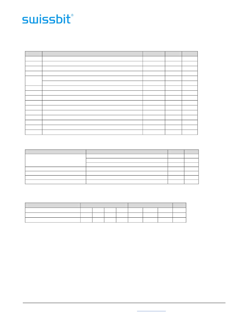
A.C. Characteristics of Temperature Sensor
V CC = 3.3 V ± 10%, T A = ?40°C to +125°C
Rev.0.9
20.09.2011
Symbol
f SCL
Parameter / Condition
SCL clock frequency
Min
10
Max
400
Unit
kHz
t BUF
t F
t R
Bus Free Time Between STOP and START
SDA fall time
SDA rise time
1300
300
300
ns
ns
ns
t HD:DAT
t H:STA
t HIGH
t LOW
t SU:DAT
t SU:STA
t SU:STO
t TIMEOUT
t I
t WR
t PU
Data hold time (accepted for Input Data)
Data Hold Time (guaranteed for Output Data)
Start condition hold time
High Period of SCL
Low Period of SCL
Data setup time
Start condition setup time
Stop condition setup time
SMBus SCL Clock Low Timeout
Noise Pulse Filtered at SCL and SDA Inputs
Write Cycle Time
Power-up Delay to Valid Temperature Recording
0
300
600
600
1300
100
600
600
25
900
35
100
5
100
ns
ns
ns
ns
ns
ns
ns
ns
ms
ns
ms
ms
Temperature Characteristics of Temperature Sensor
V CC = 3.3 V ± 10%, T A = ?40°C to +125°C
Thermal Resistance θ JA
Parameter
Temperature Reading Error
Class B, JC42.4 compliant
ADC Resolution
Temperature Resolution
Conversion Time
1
Test Conditions/Comments
+75°C ≤ T A ≤ +95°C, active range
+40°C ≤ T A ≤ +125°C, monitor range
- 40°C ≤ T A ≤ +125°C, sensing range
Junction-to-Ambient (Still Air)
Max
±1.0
±2.0
±3.0
12
0.0625
100
92
Unit
°C
°C
°C
Bits
°C
Ms
°C/W
1
Power Dissipation is defined as P J = (T J ? T A )/θ JA , where TJ is the junction temperature and TA is the ambient temperature. The thermal
resistance value refers to the case of a package being used on a standard 2-layer PCB.
Slave Address Bits of Temperature Sensor
Device
Device Type Identifier
Select Address Signals
R/W#
b7
1
b6
b5
b4
b3
b2
b1
b0
EEPROM
Temp. Sensor
1
0
0
0
1
1
0
1
A 2
A 2
A 1
A 1
A 0
A 0
R/W#
R/W#
1
The most significant bit, b7, is sent first.
Swissbit AG
Industriestrasse 4
CH – 9552 Bronschhofen
Fon: +41 (0) 71 913 03 03
Fax: +41 (0) 71 913 03 15
www.swissbit.com
eMail: info@swissbit.com
Page 12
of 15
发布紧急采购,3分钟左右您将得到回复。
相关PDF资料
SGP1200-12G
FRONT END AC/DC 1133W 12V
SL05.TCT
TVS ARRAY DATA INTFC SOT-23
SL24T1G
TVS LO CAP 300W 24V ESD SOT23
SLD10U-022-B
DIODE TVS AXIAL HI-POWER
SLP-2-413-01
SNAP LOCK PINS TEAR-DROP .413"
SLVU2.8-4.TBT
IC TVS ARRAY 4-LINE 2.8V 8SOIC
SLVU2.8-8.TBT
IC TVS ARRAY 8-LINE 2.8V 8SOIC
SLVU2.8HTG
TVS DIODE ARRAY 1CH SOT23
相关代理商/技术参数
SGN08G72G1BB2SA-DCRT
制造商:SWISSBIT 功能描述:DDR3 SO-DIMM 8 GB 1600/CL11 - Trays 制造商:SWISSBIT NA INC 功能描述:DDR3 8GB SODIMM
SGN08G72G1BB2SA-DCWRT
功能描述:MODULE DDR3 SDRAM 8GB 204SOUDIMM 制造商:swissbit na inc. 系列:- 零件状态:过期 存储器类型:DDR3 SDRAM 存储容量:8GB 速度:1600MT/s 封装/外壳:204-SO-UDIMM 标准包装:100
SGN2M056TG
制造商:Panasonic Industrial Company 功能描述:DOOR
SGN72288FH8P6PH
制造商:SMART Modular Technology Inc 功能描述:MEMORY MODULE - Trays
SGN72568FH8P0PH
制造商:SMART Modular Technology Inc 功能描述:ECC 256MX8 .94" DDR3-1333 NVDIMM - Trays
SGN72568FH8YZPH
制造商:SMART Modular Technology Inc 功能描述:2GB 1.18" MINI-NVDIMM, 256MX8 - Trays
SGN-75
制造商:EGS ELECTRICAL GROUP 功能描述:GSK 4.625X1.562X0.125 NEO
SGNE010MK
制造商:SUMITOMO ELECTRIC Device Innovations Inc 功能描述:GaN HEMTs, MK16dB, 3.5GHz, 100mA, Bulk
